第一列
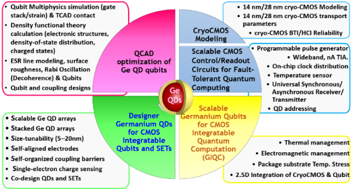
We aim to investigate and prototype scalable Ge qubits for CMOS integratable quantum computing. Using a CMOS fabrication approach, our research team has successfully realized closely-coupled Ge QDs/SiO2 shell arrays with self-aligned electrodes to interface using external test instrument at 77 K and even higher temperature. An ingenious combination of lithography and self-assembled growth has allowed us to have accurate control over the placement, shapes, and sizes of our designer Ge QDs, providing a common platform for creating QD-based qubits and single-hole transistors (SHTs) for high-temperature operation. We intend to advance our designer Ge QDs for the realization of “scalable” and “high-fidelity” Ge qubits with integrated peripheral CMOS control/readout/addressing circuitry, including programmable pulse generators, TIAs, local memory, RF-SHT readout, and auxiliary circuits (temperature sensors, universal synchronous/asynchronous receiver/transmitter (USART) addressing encoder/decoder) for fault-tolerant quantum computing.

The scopes of demonstration in this GIQC project.
-
Co-PI
-
Mau-Chung Frank Chang (National Yang Ming Chiao Tung University)
-
Chien-Nan Kuo (National Yang Ming Chiao Tung University)
-
Ying-Tsang Tang (National Central University)
Reconfigurable Germanium quantum-dot/Si-based barrier array for qubit and charge sensing
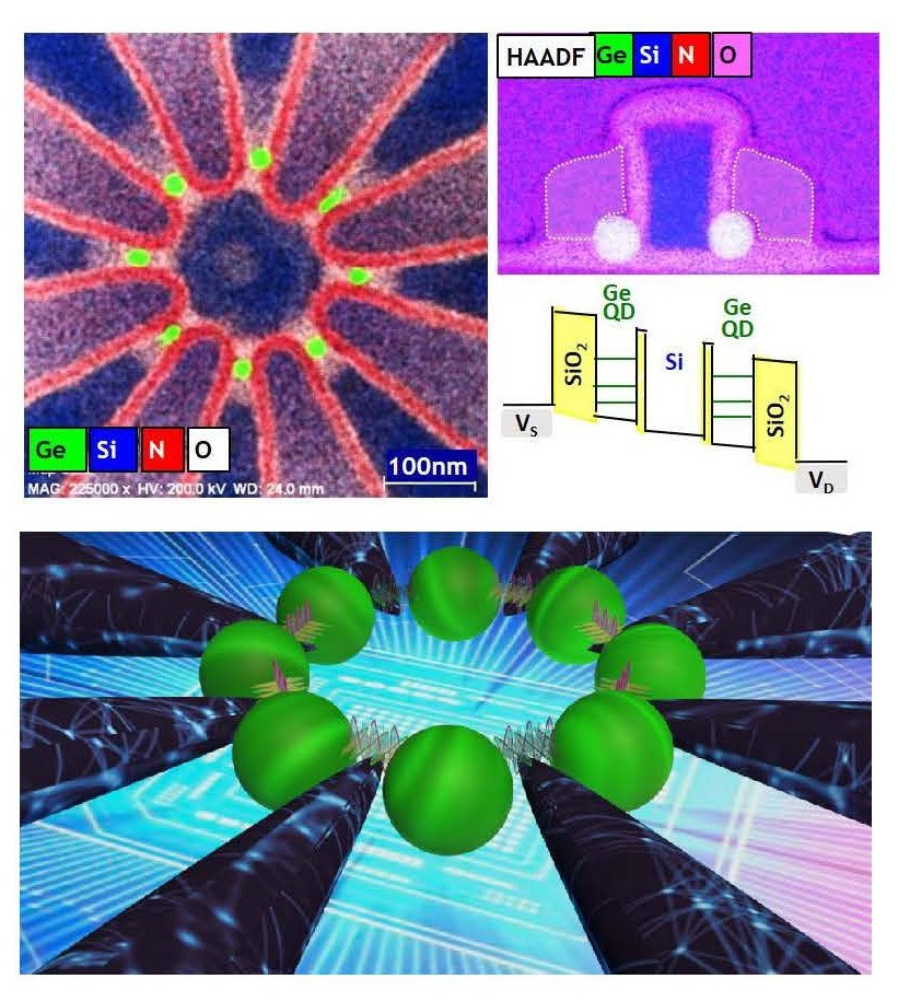
Semiconductor Si-based qubits have been realized in various lithographically-defined Si/SiGe heterostructures and validated only for milli-Kelvin temperature operation. Germanium (Ge) QD qubits systems are envisaged to have high scalabilty and operate at higher temperatures. We report the unique scalability and size tunability of Ge spherical-shaped QDs that are controllably located, closely coupled between each another, and self-aligned with control electrodes, using a coordinated combination of lithographic patterning and self-assembled growth. The core experimental design is based on the thermal oxidation of SiGe spacer islands located at each sidewall corner of Si3N4/Si fanout-ridges with specially designed fanout structures. Spherical-shaped Ge QDs are closely coupled to each other via coupling barriers of Si and to self-aligned Si-based electrodes via Si3N4 tunneling barriers. Our ability to place size-tunable spherical Ge QDs at any desired location, therefore, offers a large parameter space within which to design novel quantum electronic devices.

Reconfigurable Germanium quantum-dot array with self-organized barriers and self-aligned electrodes for quantum electronic devices.
Reference: VLSI Tech. Dig., JFS5-6, pp.1-2, June 2021
Probing charge states of Ge QDs using direct photocurrent measurement
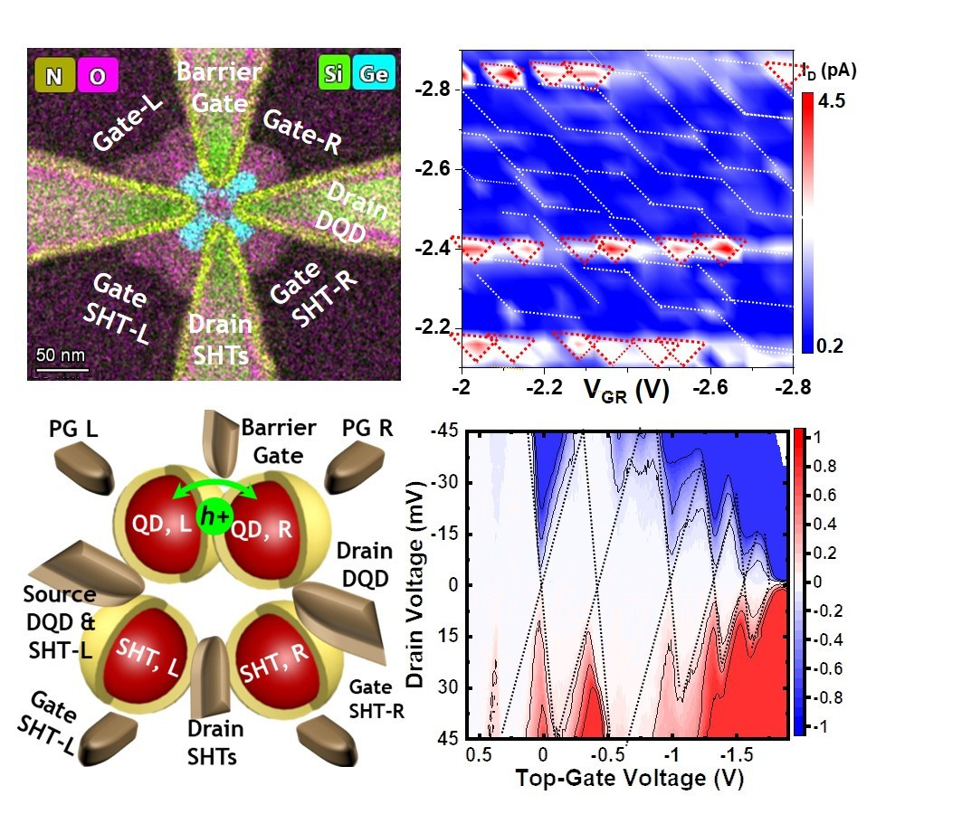
Physically-defined QDs promise higher temperature operation and better immunity to quantum leak thanks to the fact that hard-wall barriers primarily result in strong quantum confinement and enlarge energy scales. However, tunneling current through physically-defined QD qubits is typically small in magnitude (~ pA or smaller) due to strong confinement of carriers within physically-defined QDs, leading to the difficulty in resolving charge-states and their in-between transition lines simply using direct current measurement. Thereby, intricate readout techniques such as RF-reflectometry are necessary.
Our study reports that using a direct current measurement, photo-current spectroscopy of Ge DQDs not only offers a quick estimation of charging energies of the individual QDs, but also provides approximate operating conditions of charge states for further manipulation of DQD occupancy.

Photon-mediated charge transport and stability of physically-defined and self-organized germanium quantum dots/SON barriers in few-hole regime at T > 10 K
Reference: VLSI Tech. Dig., June 2024
